Quartus Prime 23.1 & Questa

Intel Quartus Prime is a software suite used for the design and synthesis of digital circuits. It is used to design, test and program FPGAs. Intel Questa is a simulation tool used to simulate digital circuits. This guide will show how to install Intel Quartus Prime Lite Edition and Intel Questa Starter Edition, how to set up the drivers for the LEGUAN FPGA board and how to simulate and synthesize a basic VHDL design.
Setup
The following steps will guide you through the installation of Intel Quartus Prime Lite Edition and Intel Questa Starter Edition. The installation process is straightforward and can be done on Windows and Linux. This guide has been written and thoroughly tested with version 23.1 of Intel Quartus Prime Lite Edition.
Downloading the installation files
Download Intel Quartus Prime Lite for either Windows or Linux here (Apple OSX is not supported). Note that while the installer application is small, it will download ~3 GB in files and require ~16 GB of storage.
Installation steps
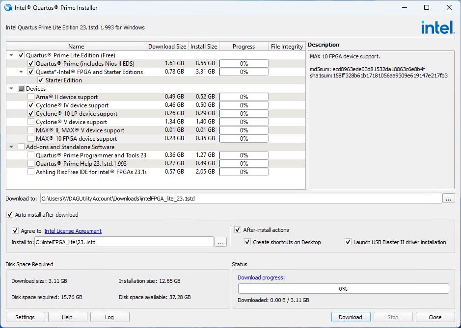
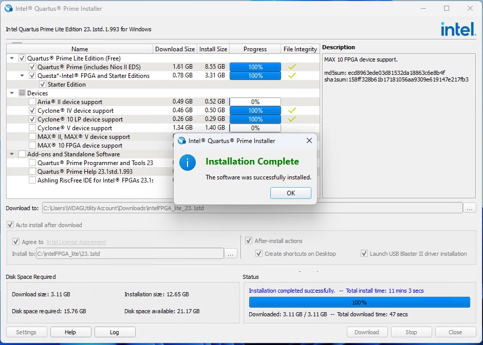
Run the downloaded installer. Ensure that
Quartus Prime,Questa Starter Edition,Cyclone IVandCyclone 10 LPare checked. Check theAuto install after download, theAgree to Intel License Agreementand theLaunch USB Blaster II driver installationoption. Once the installer has the same options checked as the image below, hitDownloadto start the installation process. Both the download and installation process may take a while.
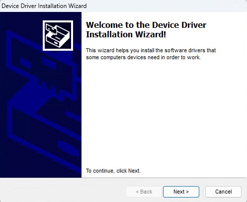
Once the Installer is finished, the Device Driver Install Wizard automatically opens. Hit
Nextto start the driver installer.
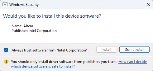
A Windows Security window will pop up. Press
Installto allow the driver installation.
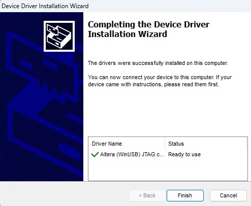
Once the installer is done, close it by clicking on
Finish.
With the driver installed, the whole installation process of Intel Quartus Prime is done. Click
OKandClosethe installer.
Post-installation steps
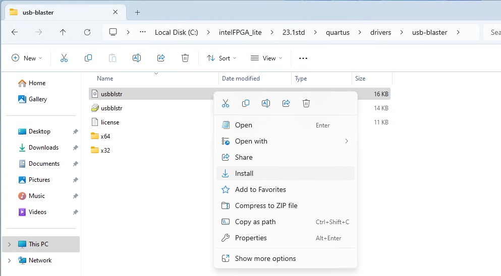
To program the LEGUAN board, the first generation USB Blaster driver has to be installed. Navigate with the Windows Explorer to
C:\intelFPGA_lite\23.1std\quartus\drivers\usb-blaster. Right-Clickusbblstr.infand selectInstall.
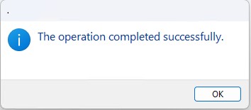
The success of the installation process is confirmed by a message window.
Plug in the LEGUAN FPGA board to the computer
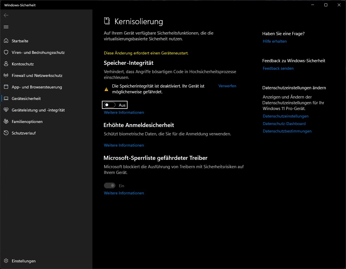
If Windows Defender Core Isolation is enabled, a warning may pop up that the driver could not be loaded on the device.
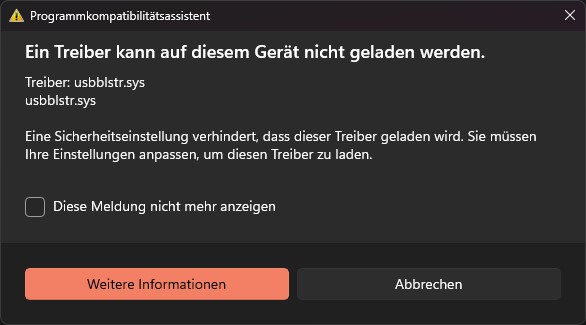
To fix this issue,
Memory Integrityhas to be disabled. Simply open this link or navigate to Windows Defender, turnMemory Integrityoff and restart the machine.
 ¨
¨
Post-installation Questa
In order to use Intel Questa Starter Edition, a license has to be requested from Intel. This guide will show how the license can be received and set up within just >20 quick steps.
Create an Intel Account on this site using the BFH credentials.
A verification code will be sent per mail. It is possible that it is caught by BFH’s mail filter. If the mail hasn’t arrived after 5 minutes, navigate to BFH’s mail filter and allow any mails from Intel.
Navigate to Intel’s License Site and click on
Enrol for Intel FPGA Self Service Licensing Center (SSLC).

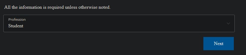
Select as profession
Studentin the drop-down menu.
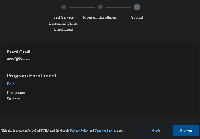
Finally submit the form. You will receive a mail in 5 to 10 minutes from Intel.
Once the mail has arrived, navigate once more to Intel’s License Site and
Sign In.

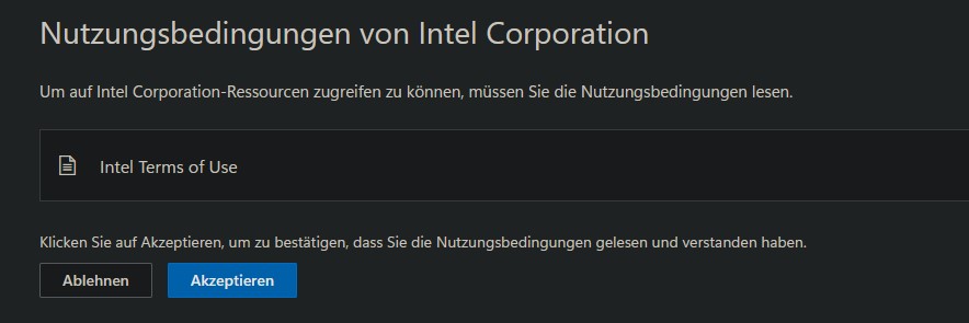
You will be requested to login with your Microsoft BFH login, add an Authenticator and link your Microsoft account with Intel. Finally, you have to accept Intel’s Terms of Use by opening the Terms and clicking on
Accept.
If you encounter the following page, wait 15 minutes and try to open Intel’s License Site and
Sign Inagain.

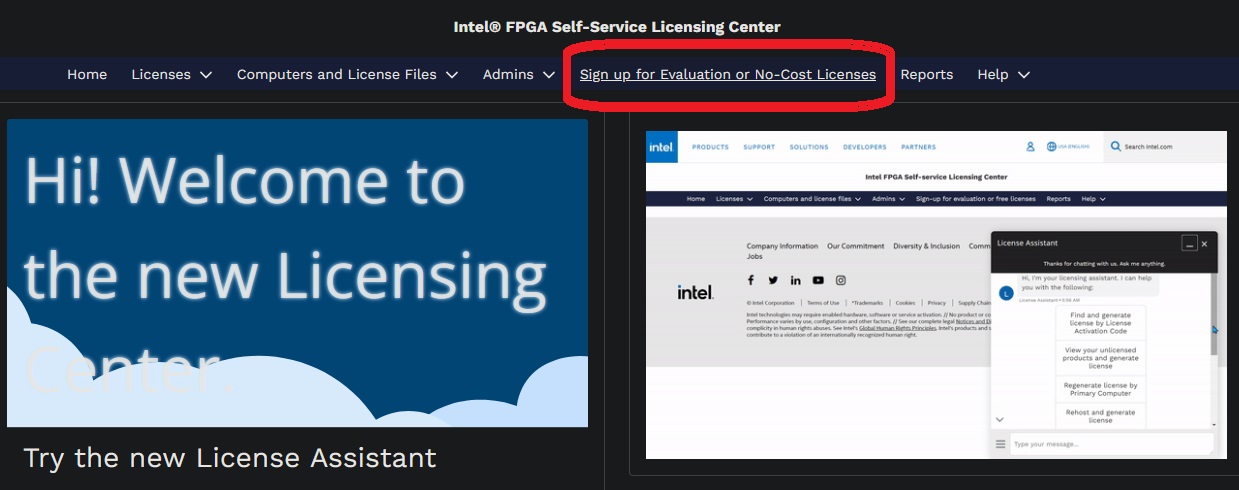
If everything went well, the following page should appear after clicking
Sign Inon Intel’s License Site. Click onSign up for Evaluation or No-Cost Licenses.
Make sure to select
Questa*-Intel FPGA Starter Edition (License: SW-QUESTA)in the list and hitNext.

Create a license by clicking on
+New Computer.
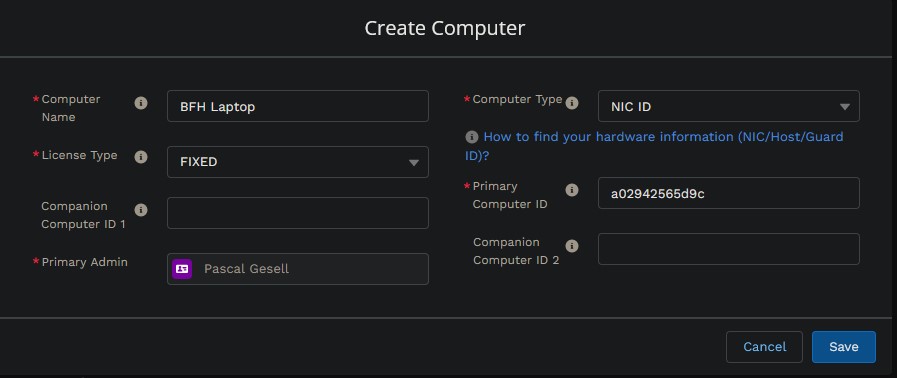
Fill out the forms as shown in the following image. Use a
Computer Nameof your choice.
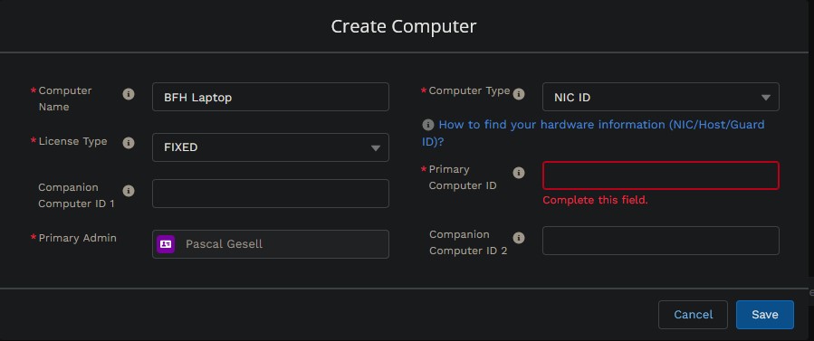
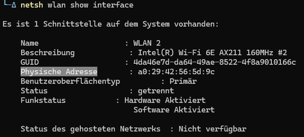
To get the
Primary Computer ID / NIC IDon Windows, openTerminaland execute the following command:
netsh wlan show interface
(If you do not have a WLAN adapter, use ipconfig /ALL and choose an physical network adapter instead)
The Physical Address of your network adapter is the
NIC IDrequired by Intel. Copy it to the form.
You will have to remove any non-hexadecimal symbols from the
NIC / Computer ID. TheIDfield should contain no more or less than 12 characters ranging from 0-9 and a/A to f/F. Click onSave.
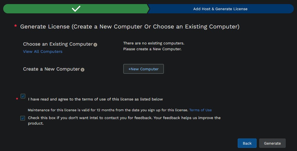
The page should look like as shown in the following image. Hit
Generateto start the license generation process.
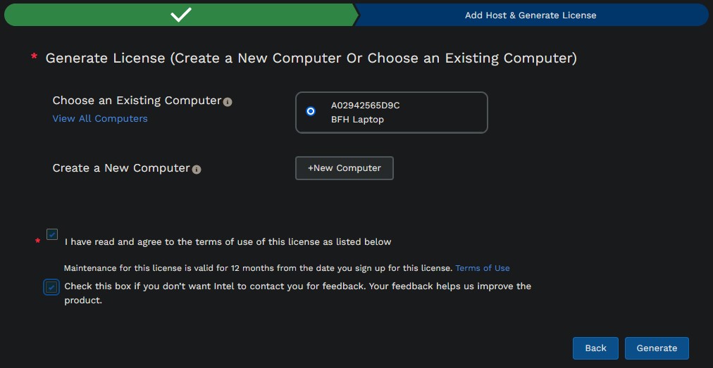
The license file will be sent per mail within a few minutes.

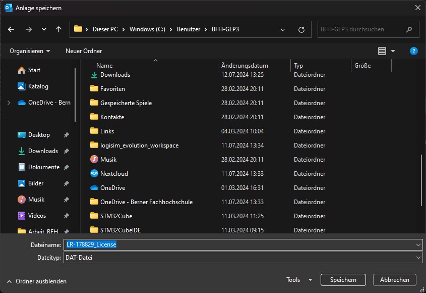
Once the mail with the attached license
.datfile has been received, save the.datfile to the computer, preferably in a location that contains no spaces or special characters in it’s path. This guide will use the base user directory.
Navigate with the Windows File Explorer to the license file, right click on it and click
Copy as Pathor pressCtrl + Shift + C.
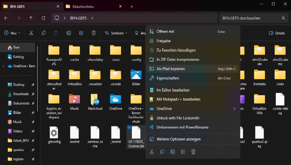
Open
Terminaland execute the following command, where PATHTOLICENSE is replaced by the path copied in the previous step (without any “ symbols):
setx LM_LICENSE_FILE PATHTOLICENSE;
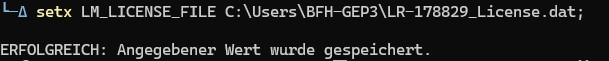
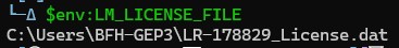
Check that the variable has been correctly saved by restarting the
Terminaland executing$env:LM_LICENSE_FILE.
Search for
Questain the start menu and openQuesta - Intel FPGA Starter Edition 2023.3 (Quartus Prime Pro 23.1std). You should see QuestaSim open up.
Testing the installation
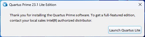
When you first launch Quartus Prime 23 Lite Edition, a window pops up to notify about their full-featured edition. Click
Launch Quartus Liteto continue.
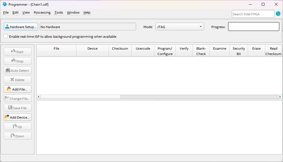
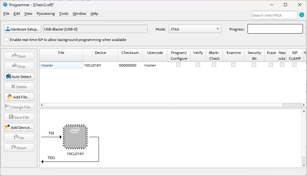
Once Quartus Prime Lite Edition is open, open the Menu
Toolsand clickProgrammer.In the Programmer window, click
Hardware Setup
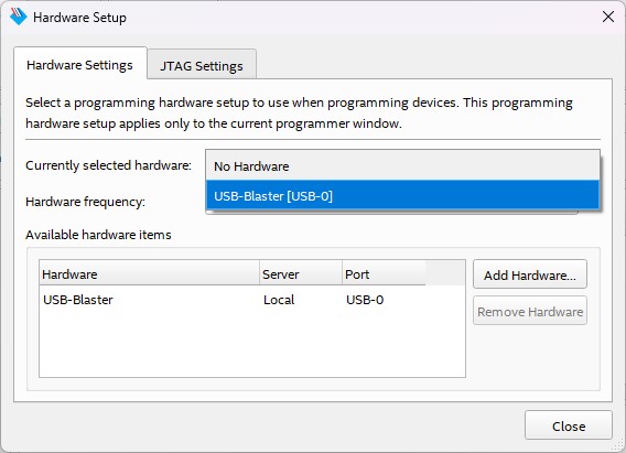
In the drop-down menu, select the
USB-BlasterandClosethe Hardware Setup Dialog.
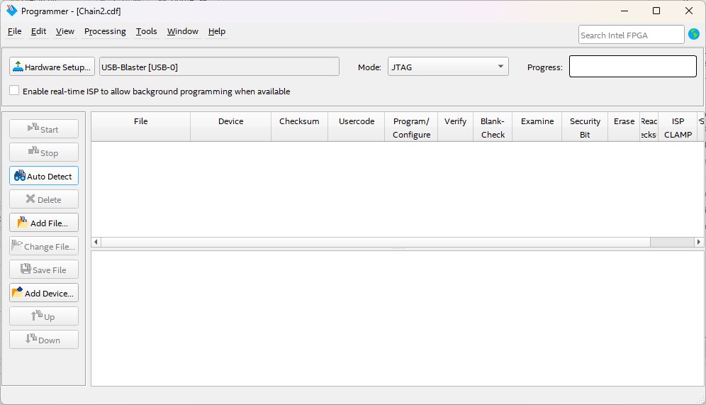
Back in the Programmer window, hit
Auto Detectto scan for the FPGA.
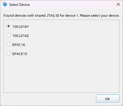
When a “Select Device” dialog pops up, make sure to select the
10CL016Ydevice and hitOK.
Congratulations, you have fully set up Intel Quartus Prime, installed drivers and connected the LEGUAN FPGA board to your machine!
Getting started with Questa & Quartus Prime
This section will guide you through the steps needed to simulate a design in QuestaSim, creating a project in Quartus Prime and loading the design on the LEGUAN FPGA board. Ensure that the previous steps were completed successfully!
For this, a basic johnson counter will be tested in QuestaSim, synthesized in Quartus Prime and loaded on the FPGA board. The ZIP archive with the required source code can be downloaded here
VHDL simulation using Questa
Before trying to synthesize VHDL to a digital circuit for download onto an FPGA, it is best to thoroughly simulate all components of your design using dedicated test benches, which apply test stimuli on your design and which may monitor automatically the output signals of the Design Under Test (DUT) for correct reactions to the stimuli. We will use Questa for this purpose, which is included in the Intel Quartus Prime Lite Edition Design Software.
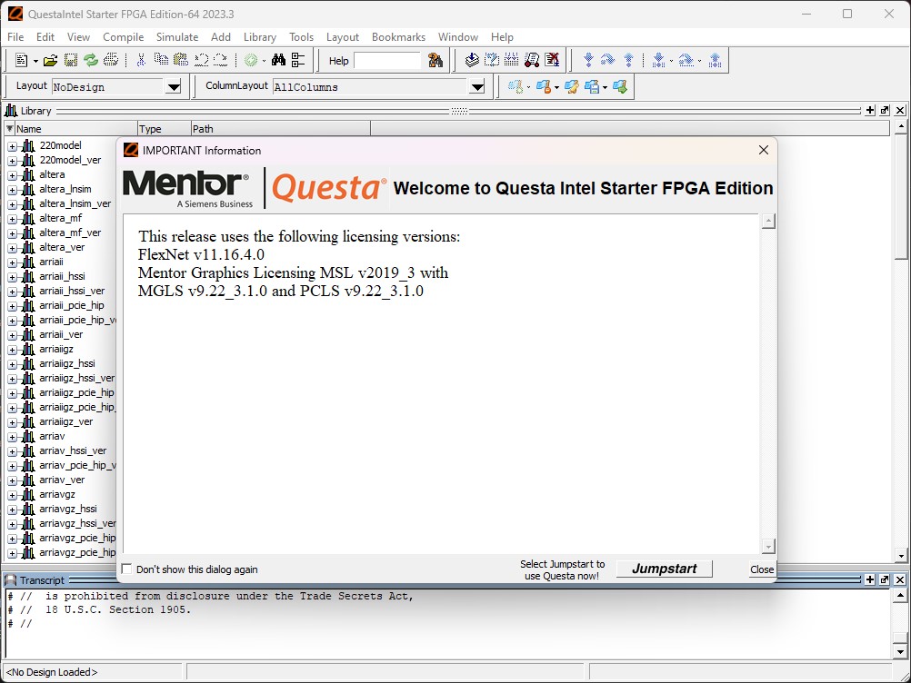
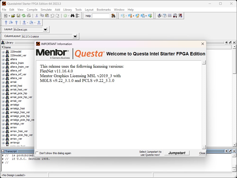
Launch Questa from the start menu by searching for
Questa.An information window will appear (similar to the one shown below). You can select the
Don't show the dialog againcheckbox if you want and click onClose.
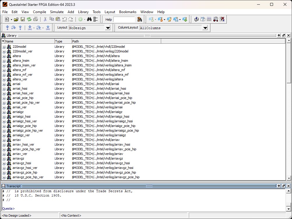
The main window of Questa is composed of a menu bar, several icon bars and initially two sub-windows: “Library” and “Transcript”. The library sub-window allows you to browse the different design libraries created by the user and provided by the Questa installation:
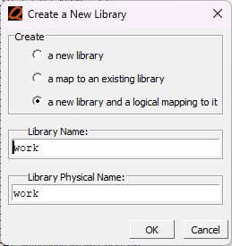
To do simulations for a project, we have to change first to the project directory. To do this, click File → Change Directory… in the menu bar and navigate to your project folder, which you extracted from the downloaded ZIP archive, and then click
Choose Directory.Now that we are in the project directory, we have to create a design library called “work” into which all models will end up that get successfully compiled. To this end, click on File → New → Library… in the menu bar. Questa will then directly offer by default in the “Create a New Library” dialog to create this work library. Click on
OKto confirm the creation of the library.
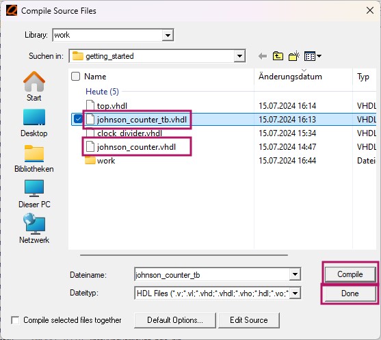
To add and compile the VHDL source files with Questa, click on Compile → Compile… in the menu bar.
The compilation of the VHDL sources has to be done in the correct order respecting the dependencies of the source files. This means that the first entities have to be compiled first, which are deeper in the design hierarchy. In our case, the compilation order is:
johnson_counter.vhd
johnson_counter_tb.vhd
Note that Questa will not automatically search for missing VHDL files in the design.
Select the files in the right order and click on
Compile. After all files have been compiled successfully, click onDoneto close the dialog.
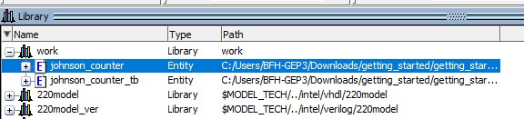
When clicking the
+sign left of the work library, you should see that the entities from the VHDL project are now part of the design library.
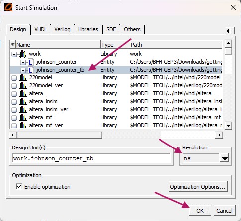
To simulate the design, click on
Simulate → Start Simulationin the menu bar. This will open theStart Simulatewindow, where the top testbench design has to be selected, as well as the simulation resolution. Setjohnson_counter_tbas the top design and set the simulation resolution tons. Click onOKto continue.
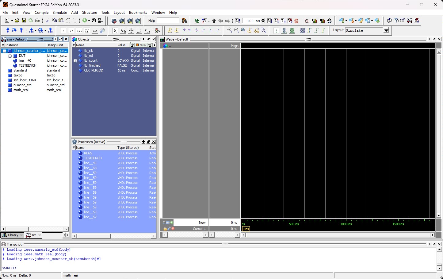
The main window has changed to the simulation layout, which contains additional sub-windows: sim, Objects, Process and Wave
The sim sub-window shows the design hierarchy, which will be simulated. That design hierarchy starts with
johnson_counter_tband contains theDUT(device-under-test) entity. TheObjectssub-window shows the signals and variables that are available in the simulation. TheWavesub-window shows the waveforms of the signals and variables that are selected in theObjectssub-window.
Make sure
johnson_counter_tbis selected in thesimsub-window. Drag & drop the signalstb_clk,tb_rst,tb_countandtb_finishedfrom theObjectssub-window to theWavesub-window. This will show the waveforms of these signals during the simulation.
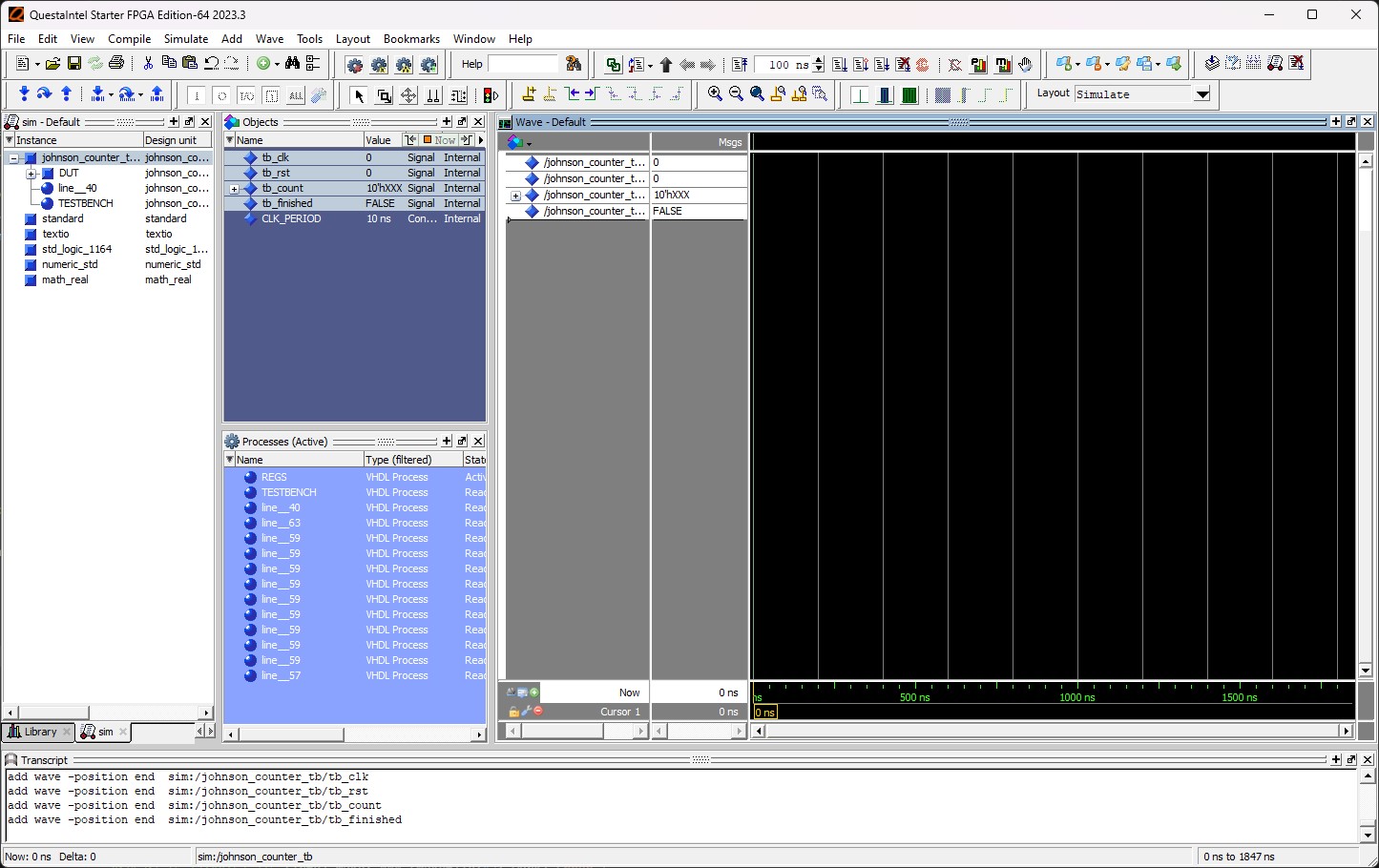
By default, Questa uses the full hierarchial name of the signals, which is a bit verbose in our case. If you click on the small, gray icon, you can toggle between the full name and the shorter, leaf-style name of the signals.
To start the simulation, click on
Run Allin the icon bar. The simulation will start and the waveforms will be displayed in theWavesub-window.
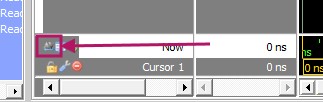
The simulation will run until no more active elements are in the test bench. To adjust the zoom of the waveforms, use either the blue magnifying glass or press the
Fkey on the keyboard.
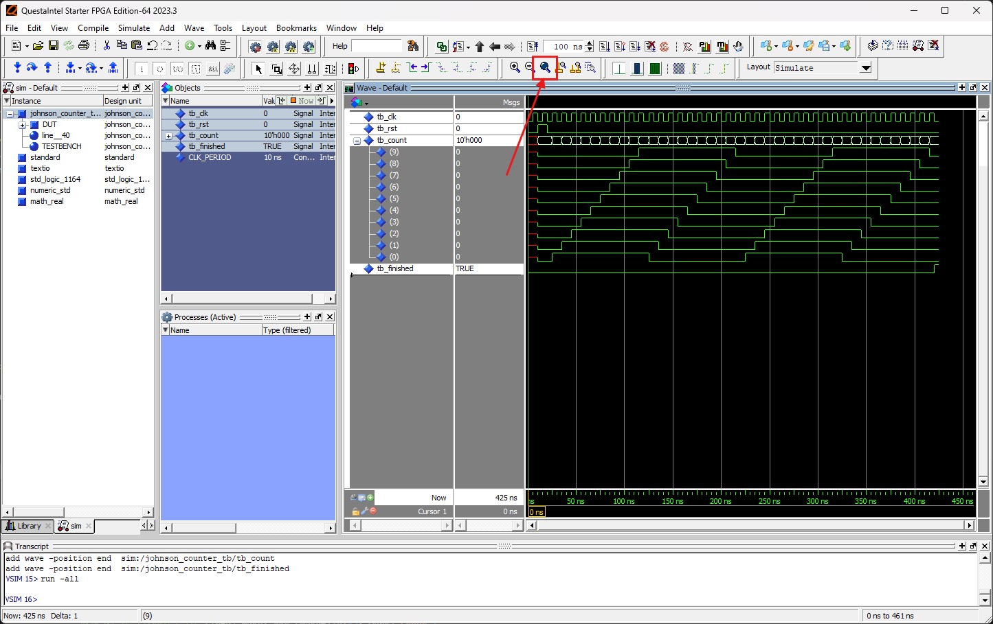
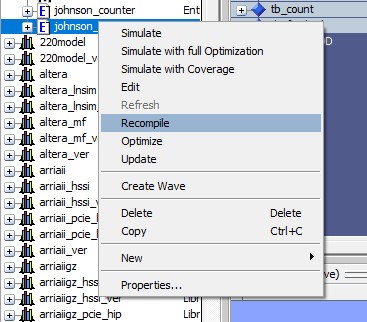
The simulation has finished successfully. You can inspect the simulation of the johnson counter and decide if the design is correct. If you want to modify the code and rerun the simulation, you can do so by clicking the
Librarytab to display the VHDL files in ourworklibrary.
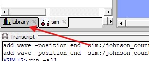
To recompile the VHDL files, simply select the files, press right-click and select
Recompile.
To restart the simulation, click on
Simulate → Restart...in the menu bar. A window will pop up, which can be confirmed by clickingOK.
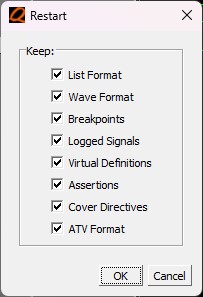
This will keep the simulation layout and selected signals, but reset the simulation and clear the waveforms. Simply click on
Run Allto start the simulation again.Congratulations, you have successfully simulated a VHDL design in Questa! You can close Questa when you are done with your simulations.
VHDL synthesis using Quartus Prime
With the design thoroughly tested in Questa, we can now synthesize the VHDL code to a digital circuit that can be downloaded onto an FPGA. This step is done in Intel Quartus Prime for the LEGUAN FPGA board.
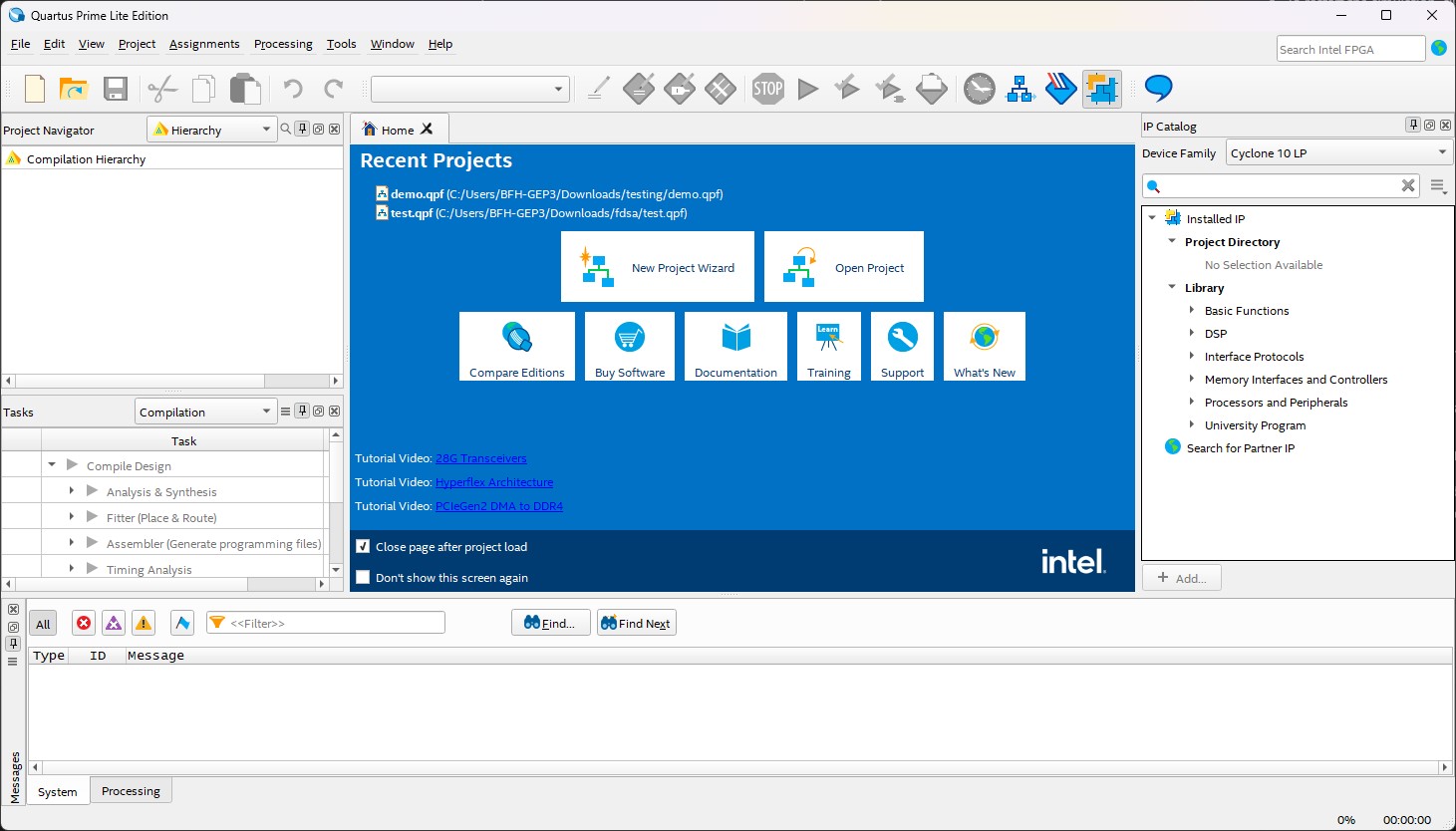
Launch Quartus Prime from the start menu by searching for
Quartus Primeand starting it. After the start, the main window looks like this.
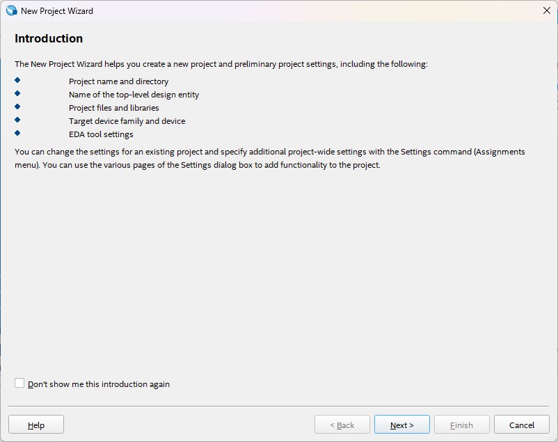
To create a new project, click on
New Project Wizardin the start screen. This will open theNew Project Wizardwindow. Click onNextto continue.
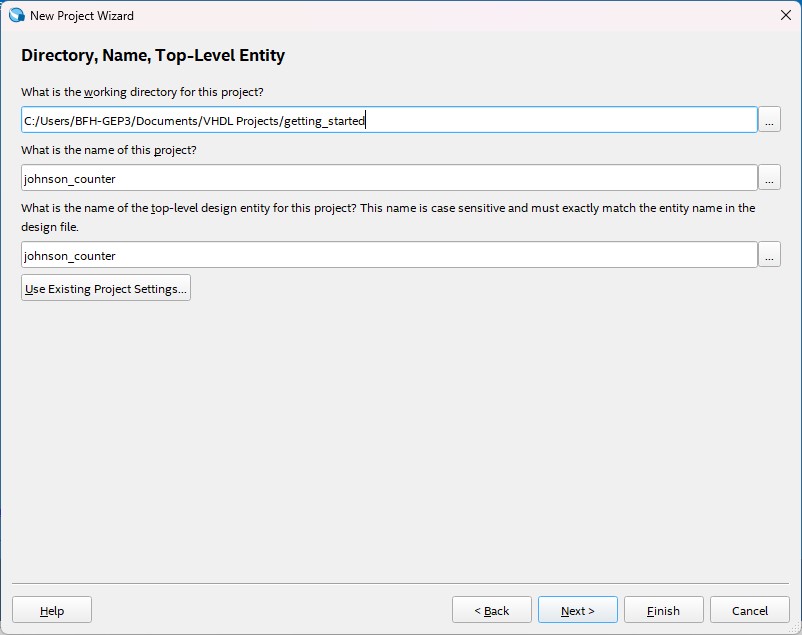
Set the project directory as the location of the VHDL project files. This is the directory where you extracted the ZIP archive. Use a fitting project name, such as
johnson_counterand click onNext.
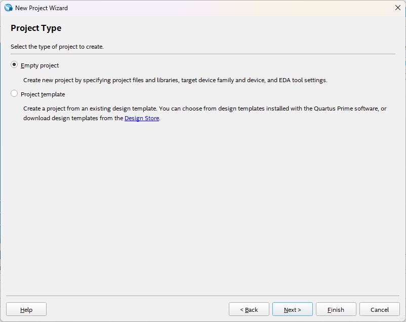
Select the
Empty Projecttemplate and click onNext.
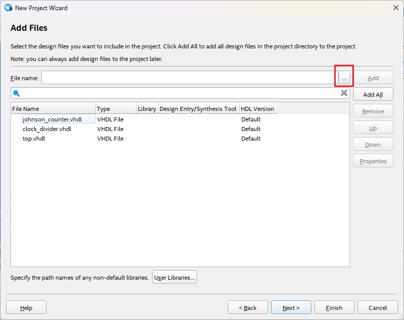
Add the VHDL files to the project by clicking on
.... Select the VHDL filesjohnson_counter.vhdl,clock_divider.vhdlandtop.vhdland click onOpen. After the files have been added, click onNext.
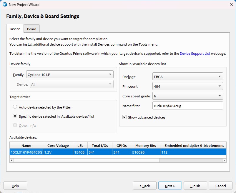
Choose the correct FPGA family and device. In our case for the LEGUAN FPGA board, use the name filter with
10CL016YF484C6G, click on the device in the list and click onNext.
Make sure that the
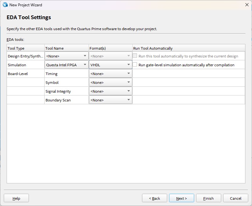
Simulationis set toQuesta Intel FPGAand the format toVHDL. Click onNext.
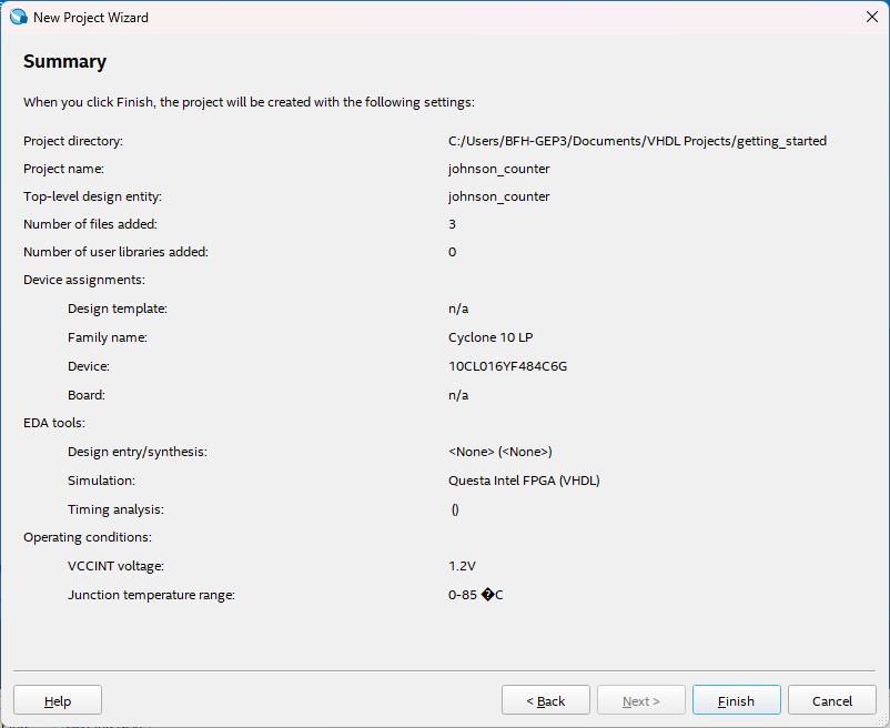
Click on
Finishto create the project.
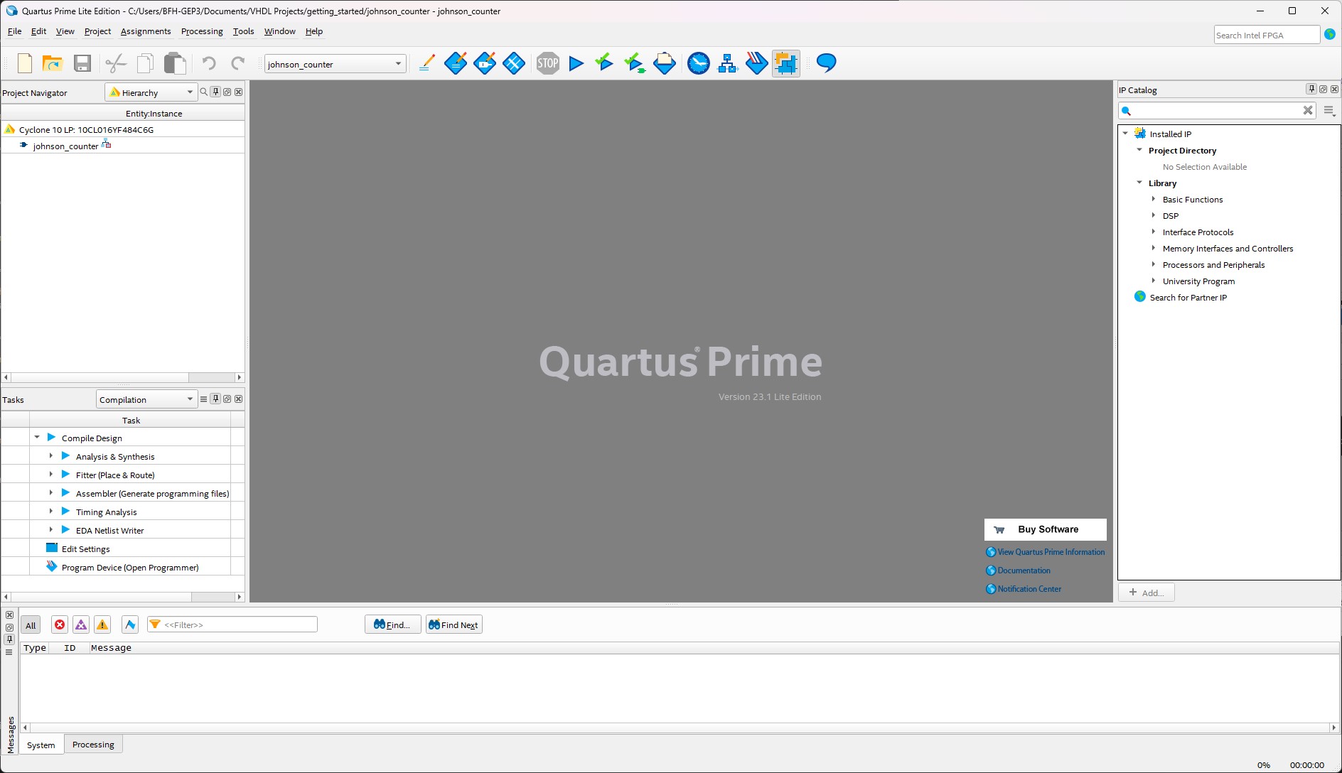
Quartus Prime should look now like this .
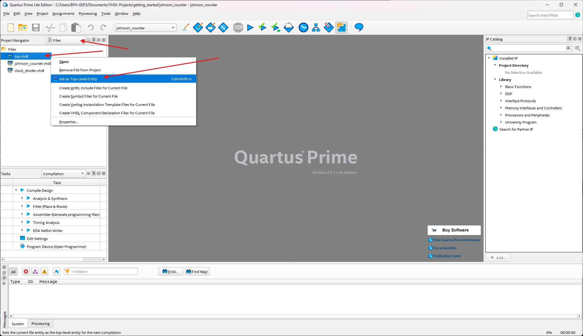
Make sure the
top.vhdlis the top entity of the design. For this, change theProject Navigatorto display theFiles, right-click ontop.vhdland selectSet as Top-Level Entity.
To start the synthesis, either click in the Task
Compile Design → Analysis & Synthesisor click on the corresponding icon in the top icon bar.
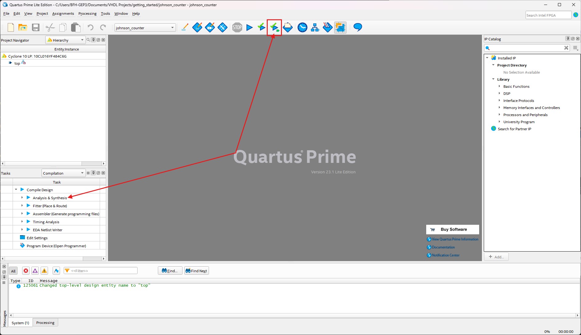
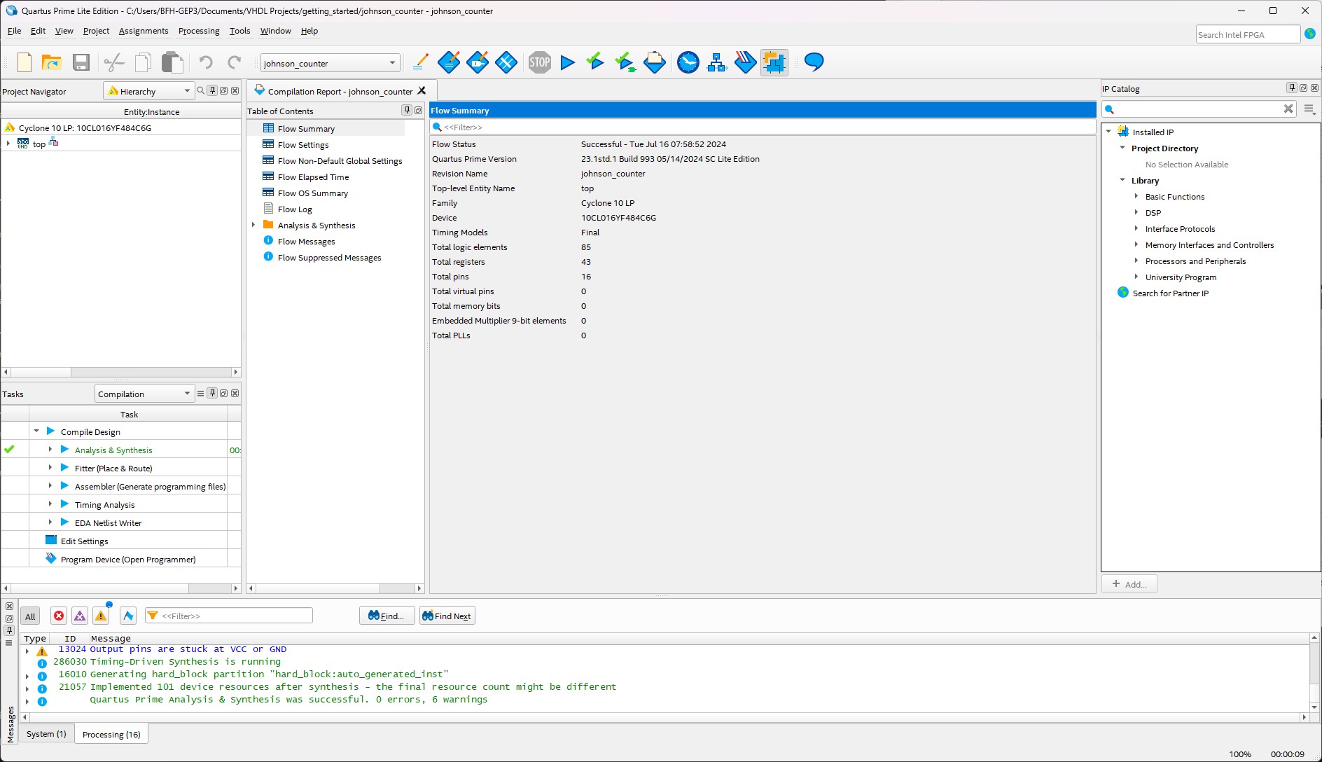
Quartus will show the progress at the bottom and print out any errors or warnings in the
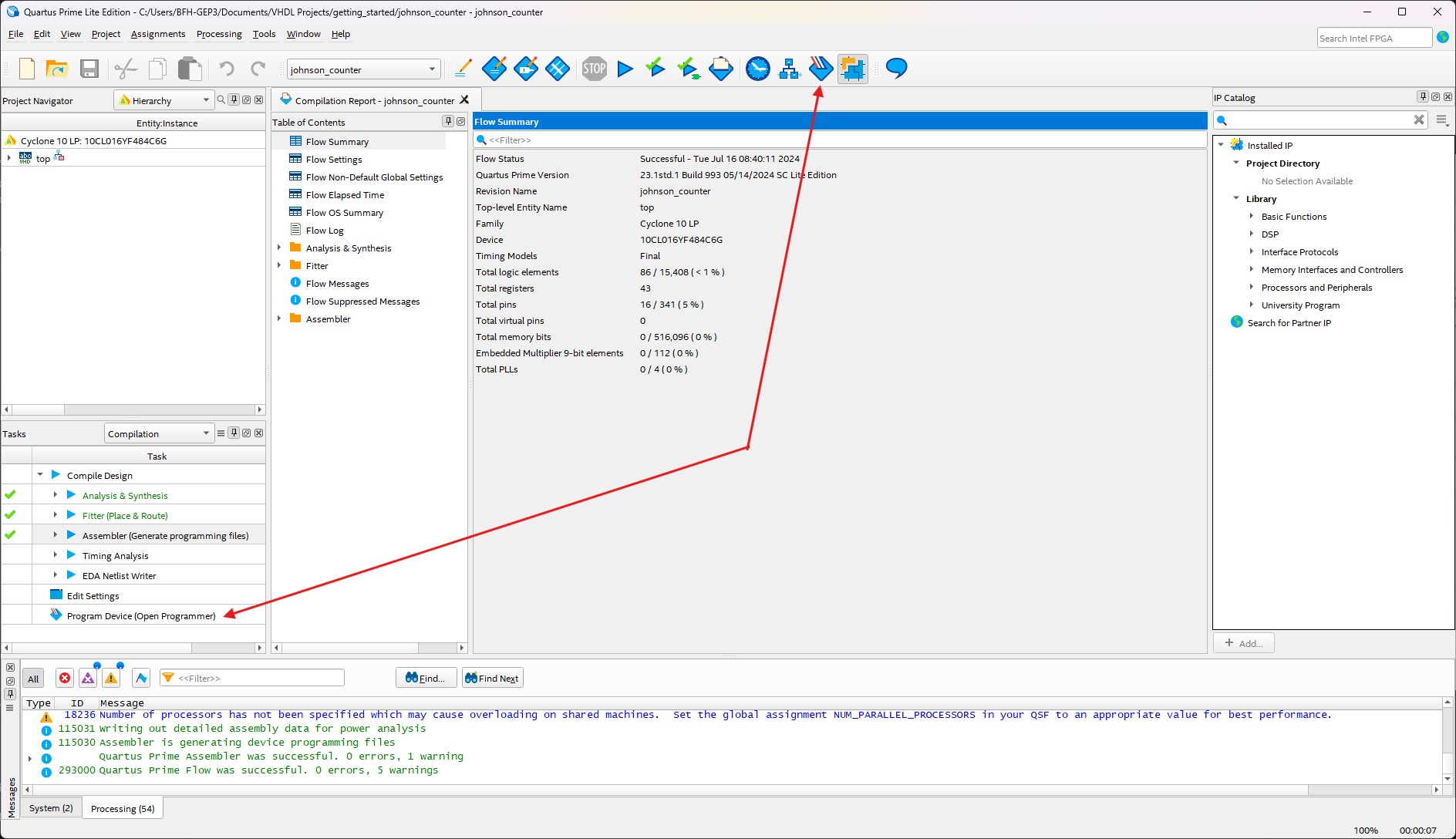
Messageswindow. If the synthesis was successful, theFlow Summarywill show the resource usage of the design and the hierarchy of the design is displayed in the Project Navigator → Hierarchy pane.
The logic circuit, that Quartus extracted from the VHDL code, can be viewed by clicking on the task
Compile Design → Analysis & Synthesis → Netlist Viewers → RTL Viewer. Each entity can be opened by clicking on the+to show it’s actual realization up to the gate level.
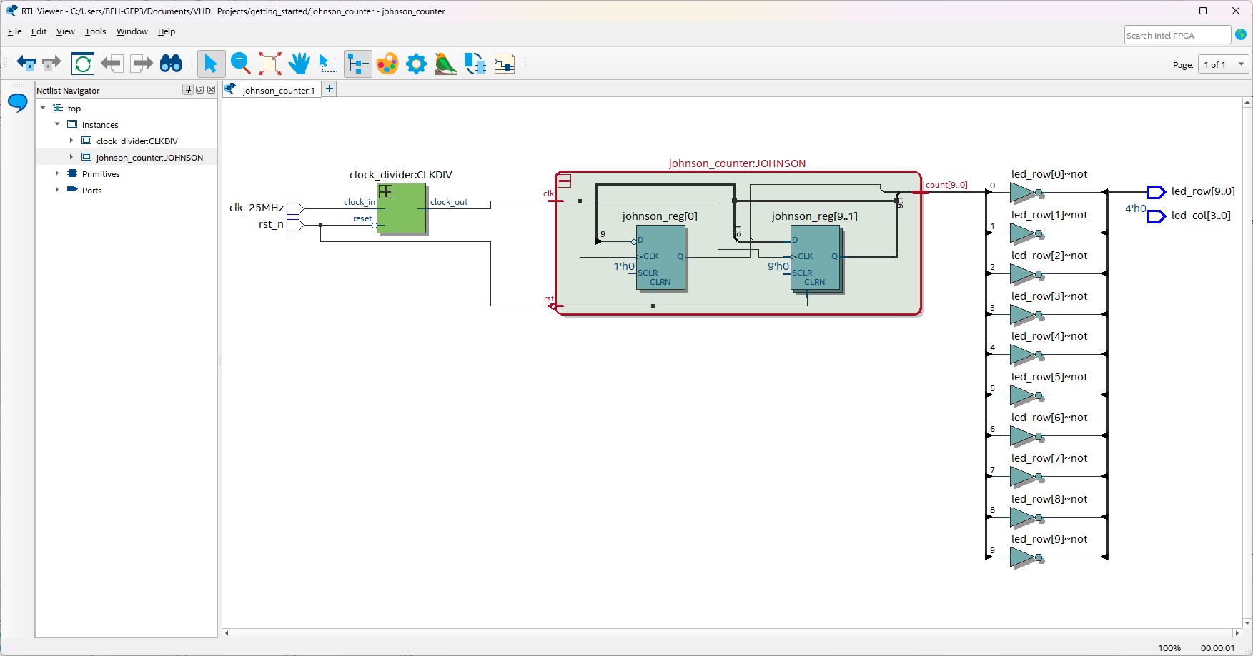
Compare the design to the VHDL code. After you are done, close the RTL Viewer.
To see how the design will be actually mapped on the FPGA, click on the task
Compile Design → Analysis & Synthesis → Netlist Viewers → Technology Map Viewer.
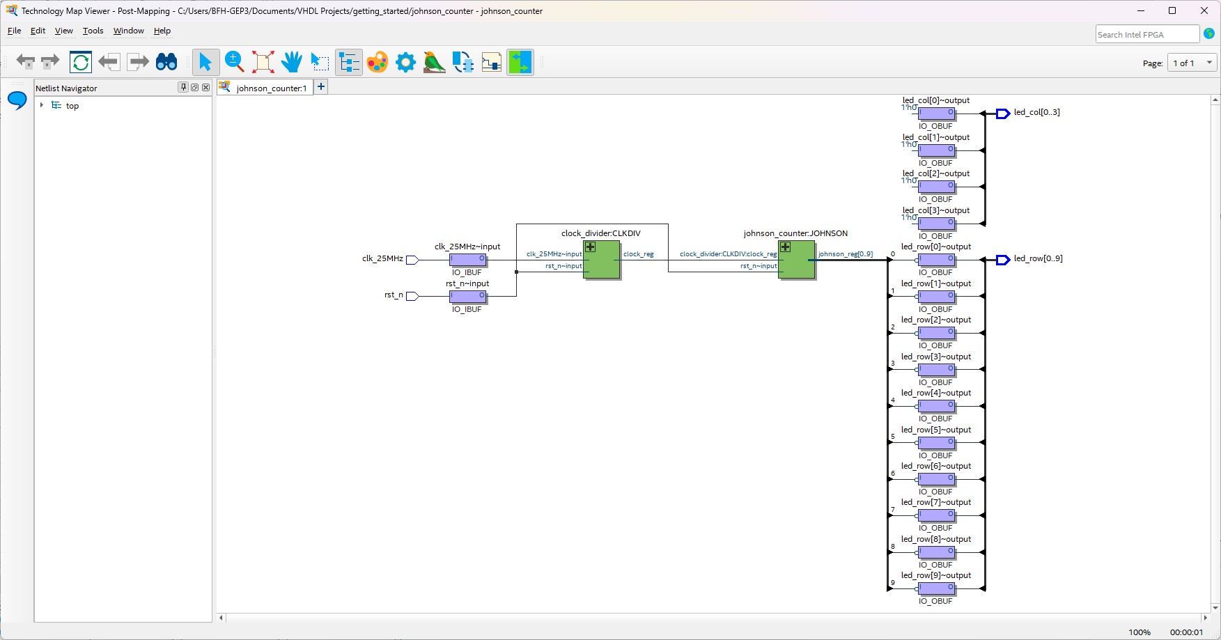
The Technology Map Viewer shows the actual mapping of the design to the FPGA. Each entity can be opened by clicking on the
+to show it’s actual realization up to the gate level. After you are done, close the Technology Map Viewer.Before the design can be downloaded onto the FPGA, a pin assignment has to be done. This is done by clicking on the task
Compile Design → Analysis & Synthesis → I/O Assignment Analysis → Pin Planner. At the bottom, all the signals from the TOP file are displayed. The pin assignment can be done by typing the PIN of the FPGA in theLocationfield of every signal.
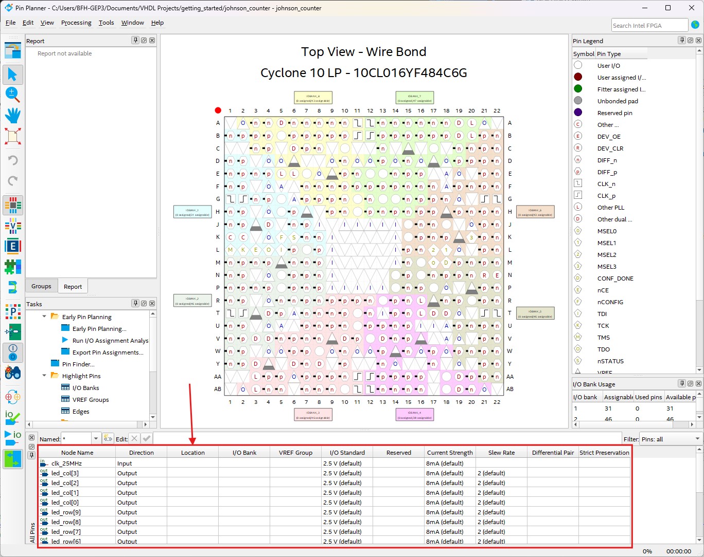
While every pin on the FPGA starts with the prefix
PIN_, it’s enough to just type in the connection without thePIN_(Instead of typingPIN_B11, just typeB11into the location). To get the pin location of buttons and LEDs, simply navigate to the FPGA section of this wiki. Assign the following pins to the signals:
| Signal | Pin | Comment |
|---|---|---|
| clk_25MHz | PIN_B11 | 25 MHz clock signal |
| led_col[3] | PIN_E21 | LED column signals |
| led_col[2] | PIN_E22 | LED column signals |
| led_col[1] | PIN_F21 | LED column signals |
| led_col[0] | PIN_M22 | LED column signals |
| led_row[9] | PIN_Y21 | LED row signals |
| led_row[8] | PIN_W21 | LED row signals |
| led_row[7] | PIN_V22 | LED row signals |
| led_row[6] | PIN_U22 | LED row signals |
| led_row[5] | PIN_R21 | LED row signals |
| led_row[4] | PIN_P21 | LED row signals |
| led_row[3] | PIN_M20 | LED row signals |
| led_row[2] | PIN_F17 | LED row signals |
| led_row[1] | PIN_K17 | LED row signals |
| led_row[0] | PIN_J17 | LED row signals |
| rst_n | PIN_A11 | Reset signal |
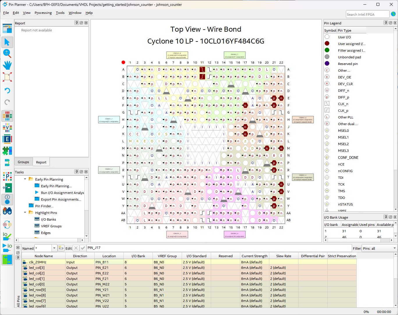
After the pin assignment is done, close the Pin Planner. Before the design can be downloaded onto the FPGA, the Fitter and the Assembler have to be run to generate the bitstream for the FPGA. This is done by clicking on the task
Compile Design → Assembler (Generate programming files)(This will run the Fitter and the Assembler. If the design needs to be recompiled, it will too be automatically done).
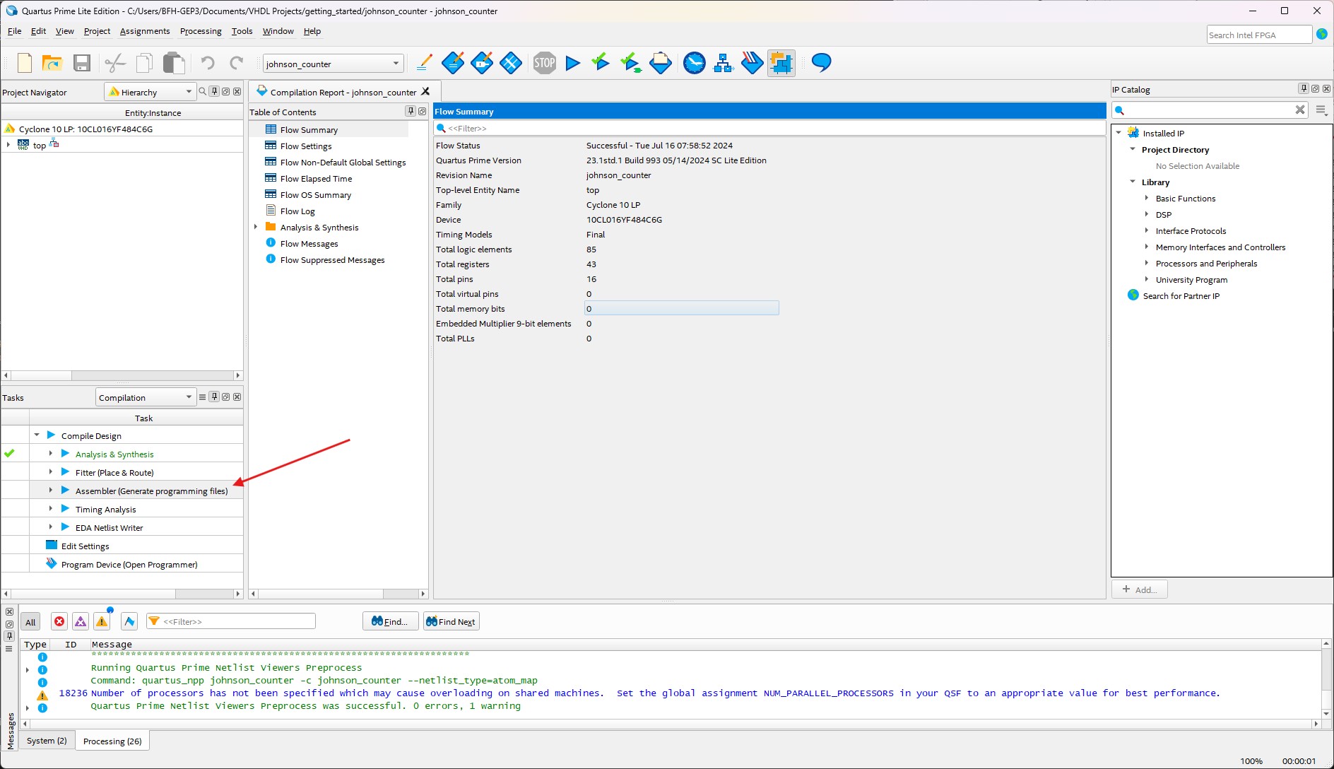
Once the Assembler has finished, the flow summary will show the resource usage of the design. With the bitstream generated, it can be loaded onto the FPGA by double-clicking on the task
Program Devicein theTaskswindow or by clicking on the corresponding icon in the top icon bar.
Connect the LEGUAN FPGA board to the computer and make sure the
FPGA without LCDmode is active. Click onHardware Setup, select theUSB-Blasterand click onClose. SelectStartto load the bitstream onto the FPGA.
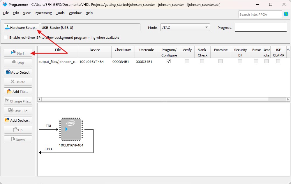
The bitstream will be loaded onto the FPGA. Once the process is finished, the LEDs on the FPGA should show the output of the johnson counter.
Congratulations, you have successfully synthesized a VHDL design in Quartus Prime and loaded it onto the FPGA! You can close Quartus Prime when you are done.
Conflicts with Analog Discovery 2
Note: This section is only relevant for Windows users.
Make sure to disconnect the Analog Discovery 2 from the computer when using Intel Quartus Prime. The Intel Quartus Prime software has issues detecting the Altera USB Blaster when the Analog Discovery 2 is connected. This is a known issue and currently, this is the best workaround. After the new bitstream has been programmed, the Analog Discovery 2 can be connected again.